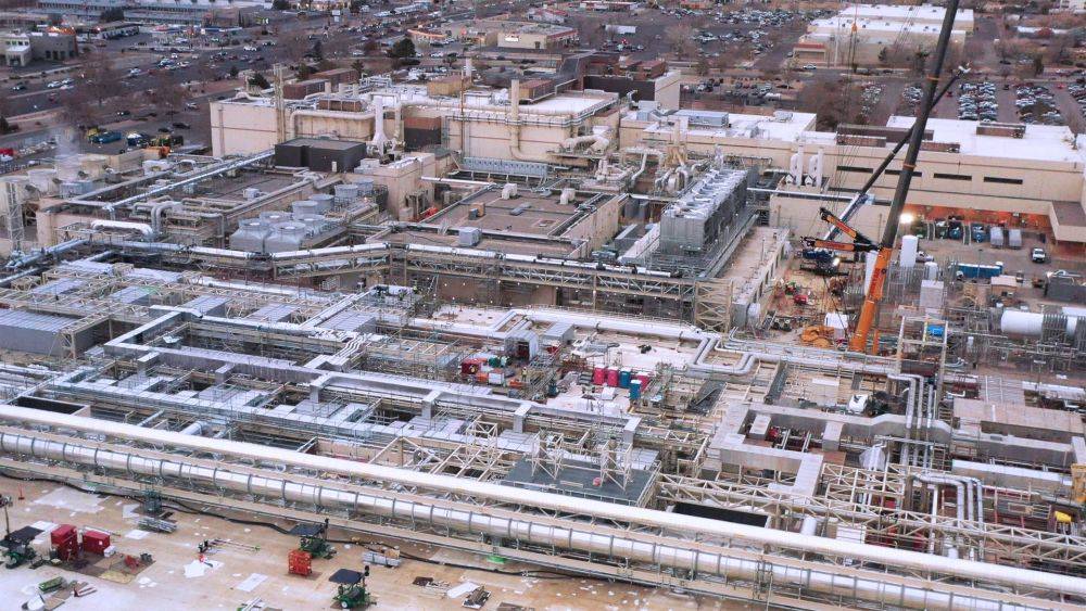
There are few easy ways to get across the incredible complexity required to build a modern computer chip: this photograph is one of them
Chipmaking is tough. Like really tough. Just how tough? An engineer could spend many hours talking about the intricacies of just a single step in the lithographic or packaging process and you'd come away wiser but moderately terrified about the scale of the accomplishments required to create any and all computer chips. But a photograph speaks a thousand words, and these photos of Intel's new lithographic 'High NA EUV' machines make it quite clear how incredibly complex this whole chipmaking biz is.
What you're looking at here is a lithography tool (just one, incredibly) called a TWINSCAN EXE:5000 High NA EUV. This $370 million machine offers Intel the new ability to scale down processors into more efficient, effective designs. 'High NA' stands for High Numerical Aperture. 'EUV' stands for Extreme Ultraviolet.
The wider chipmaking industry has been adopting EUV to allow for more continued advancement of chipmaking. Previous DUV lithographic processes only go so far, and the smaller chips are required to go, the more DUV processes are required to introduce extra steps into the manufacturing process, such as multi patterning. This adds time, complexity, and cost. That's where EUV comes in, which reduces the number of processes required again while allowing for sub-10nm process nodes. In theory, this also reduces cost, though in practice hasn't worked out that way. EUV requires extremely large and complicated tools, as you might be able to tell from the photographs below.
The important thing is it remains possible to make more complicated and better performing processors thanks to EUV. Intel uses EUV within its Intel 4 process node. TSMC has used EUV since N7+.
High NA EUV is a little different again. Using newer machines from ASML, the company that makes most lithographic machines out of the Netherlands, Intel is able to produce wafers quicker and enjoy higher yields per wafer (a higher proportion of processor on each wafer are usable). Mark Phillips, an Intel Fellow
Related News


