TSMC Starts Preparing For 1nm Production, Plans For a Cutting-Edge Facility In Taiwan
The semiconductor giant TSMC preps for 1nm production, as the firm starts planning the development of a cutting-edge fab in Taiwan.
TSMC Ventures Into Cutting-Edge 1nm Production, Total Development Costs To Exceed $32 Billion Mark
TSMC has just made the semiconductor race much more interesting since the company has become the world's first foundry to start preparing for 1nm production. This is indeed a new benchmark for the industry since the 1nm segment is known to be the "holy grail" in the domain of semiconductors, and as always it looks like the Taiwanese giant will take the lead here, surpassing the likes of Intel and Samsung Foundry. The new facility, which is expected to be developed in Chiayi County, southern Taiwan, would bring a revolution to the tech industry, in terms of performance and efficiency gains.
Related Story TSMC’s Shares Blossom After A.I. Focused Analyst Call Draws Management Confidence
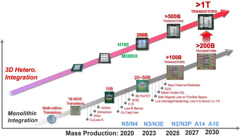
Before we go into the crux of the proposed facility, let's take a brief look at TSMC's 1nm process. Back in the IEDM conference, TSMC shared its plans to develop the 1nm node by 2030, and interestingly, the firm showed optimism to integrate a whopping "trillion transistors" on the process, through multiple 3D-stacked chipsets. TSMC has sort of changed its naming scheme after 2nm, with 1.4nm and 1nm processes being labeled as A14 and A10, showing some resemblance with Intel Foundry. However, success lies in how TSMC achieves this goal, especially because yield rates and supply have been a huge problem for the semiconductor industry in recent times.
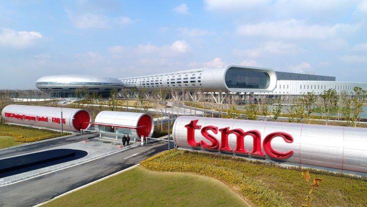
Taiwan Economic Daily discloses that TSMC's plans for 1nm would be a pricey one, with estimated costs exceeding the one trillion won figure, or around $32 billion. The facility is expected to be built at Southern Taiwan Science Park (STSP), with an estimated size of 100 hectares, which would be divided into a 60-40 ratio, to cater to both semiconductor and IC packaging production within the new facility. TSMC is also
Related News


