TSMC Ready For The Angstrom-14 Era, Initiates Development On Cutting-Edge 1.4nm Process
TSMC has announced that the firm has finally entered the "Angstrom 14 Era" as they initiate development on their cutting-edge A14 process.
TSMC Doesn't Look To Slack Behind Competition At All, 1.4nm "Angstrom" Nodes To Drop By Within The Next Five Years
TSMC released its Annual Report 2023 a few months ago, but apparently, the documentation contained crucial information that was missed. Before we dive into that, let's talk a bit about TSMC's A14, or what is labeled as a tech revolution by many analysts out there.
Related Story Apple Rumored To Be Developing Custom Silicon For AI Servers, New Chip Said To Use TSMC’s 3nm Process And Will Enter Mass Production In 2025
Right now, we are on the timeline for TSMC's 3nm processes to start to see widespread adoption. Hence, the 1.4 nm still has a lot way before it debuts into the markets and will likely come after 2nm and 1.8nm nodes, which means that you can expect it to drop at least within the next five years or maybe more.
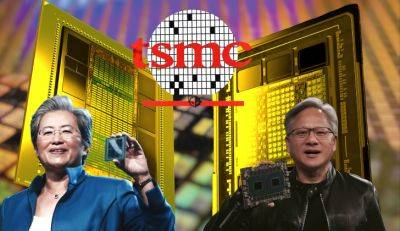
Moving on to the more interesting tidbits, prominent analyst Dan Nystedt has managed to dig into TSMC's documents, extracting information about the firm's 1.4nm process, as disclosed to investors in their annual report. TSMC says that their 1.4nm node is targeted towards high-end SoCs and HPC applications, likely indicating that their primary focus is indeed getting distributed from traditional mobile and computing markets to the AI segment as well. TSMC says that they will likely explore the next-generation EUV scanners for the A14 process, which means that it is still in the R&D stages.
Moreover, the Taiwan giant says that they have moved to "exploratory studies" for nodes beyond 14A, which is mere speculation for now. Still, they are likely talking about 1nm and ahead if process shrinking becomes the way to move forward after a decade or so. TSMC expects to significantly bump up its R&D expenditures in the coming years after already witnessing an 11.7% YoY increase in the R&D budget, and the firm
Related News


