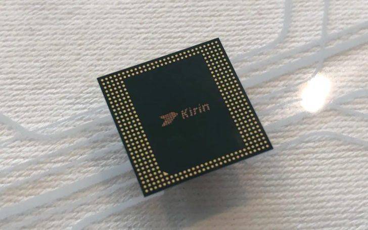
Huawei’s Mate 70 Series May Not Use The First SMIC 5nm Chipset, But A More Refined ‘N+3’ Node With a Higher Density Than Kirin 9010
The Kirin 9000S that allowed Huawei to break free of the U.S. trade ban was mass produced on SMIC’s 7nm (N+2) technology, with the company maintaining its momentum with the Kirin 9010 that is found in the Pura 70 series. For the Mate 70 range, rumors have disseminated in multiple directions, with whispers claiming that the former Chinese giant would use SMIC’s 5nm process that the semiconductor manufacturer reportedly developed successfully. However, there appears to be a twist in Huawei’s plans, with one rumor stating that the next Kirin SoC powering the Mate 70 series would be mass manufactured on SMIC’s N+3 process, which touts a higher density compared to the N+2 variant.
New Kirin SoC could be limited to SMIC’s 7nm process but sporting higher transistors, leading to some advantages over previous chipset releases
The Mate 70 series has previously been rumored not to transition to SMIC’s 5nm process, with the Kirin 9100 expected to be retained at 7nm. While that sounds incredibly disappointing, there were likely practical reasons for this decision, assuming Huawei has already made its. Mass producing 5nm wafers on the older DUV machinery instead of EUV equipment means that production costs will be high and yields will be low.
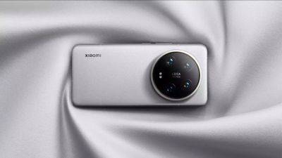
Related Story Huawei’s Pura 70 Series Boosts The Company’s Annual Shipments By 125 Percent, New Lineup More Popular Than Last Year’s P60 Range
In short, the cost of each 5nm wafer coming out of SMIC’s production site will be highly expensive, so Huawei probably believes that the costs do not justify using this technology for its smartphone chipsets. This setback means that the Kirin 9100 could be fabricated on the 7nm process, but using the N+3 node, it could boast a higher density than the Kirin 9010 and the Kirin 9000S. This improvement means that the Kirin 9100 will boast a higher number of transistors, resulting in better ‘performance per watt’ and improved power efficiency.
In addition to the upcoming chipset powering the Mate 70 family,
Related News


