Huawei Has Reportedly Invested Billions In An R&D Facility That Will Allow It To Develop Advanced Chipmaking Machinery Similar To ASML & Others
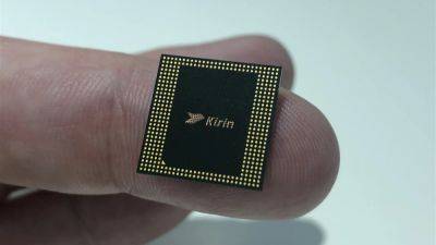
SMIC and Huawei might have successfully developed the 5nm process for future chipsets, but there is a technological ceiling that the Chinese firm cannot phase through if it continues to rely on existing DUV machinery. With no way to get its hands on cutting-edge EUV chipmaking tools from companies like ASML, a new report states that Huawei is taking matters into its own hands, and that is by heavily investing in an R&D facility with the sole purpose of making advanced machinery similar to those produced by leading companies.
When completed, Huawei’s advanced R&D facility is said to cover an area of 224 football fields
The U.S. trade ban has put Huawei on a path of self-sufficiency, but the road will be full of potholes, roadblocks, and other obstacles, not to mention the intense capital that the company’s route will require. According to Nikkei, a new R&D center near Shanghai is being constructed, with the main goal being to develop chipmaking tools that will be competitive with the machines made by ASML, Canon, and Nikon. Currently, Huawei’s foundry partners SMIC and Hua Hong are barred from purchasing tools that allow them to make chips on the 14nm FinFET and 16nm FinFET processes.
Related Story Huawei Witnessed A Stellar 42 Percent Annual Phone Shipments Growth During China’s 618 Sale, Despite Offering Fewer Discounts Than Apple And Other Brands
Instead, both semiconductor manufacturing firms can only get their hands on the 28nm lithography systems, putting them at a severe disadvantage when compared with the United States. The other problem is that 90 percent of this market is controlled by ASML, which is why Huawei is pursuing this R&D facility development. So far, the company has invested approximately ¥12 billion, or $1.66 billion, and when completed, its area will be equivalent to 224 football fields and house over 35,000 employees. Also, Huawei is said to have offered attractive salary packages to acquire top talent in the field of semiconductors.
However,
Related News


